Kentsfield

Sunday, July 19, 2009


The Kentsfield released on November 2, 2006 was the first Intel desktop quad core[26] CPU branded Core 2 (and Xeon for lower-end servers and workstations). The top-of-the-line Kentsfields were Core 2 Extreme models numbered QX6xx0, while the mainstream ones branded Core 2 Quad were numbered Q6xx0. All of them featured two 4 MB L2 caches. The mainstream Core 2 Quad Q6600, clocked at 2.4 GHz, was launched on January 8, 2007 at US$851 (reduced to US$530 on April 7, 2007). July 22, 2007 marked the release of the Q6700, and Extreme QX6850 Kentsfields at US$530 and US$999 respectively along with a further price reduction of the Q6600 to US$266.[27]

Analogous to the Pentium D branded CPUs, the Kentsfields comprise two separate silicon dies (each equivalent to a single Core 2 duo) on one MCM.[28] This results in lower costs but lesser share of the bandwidth from each of the CPUs to the northbridge than if the dies were each to sit in separate sockets as is the case for example with the AMD Quad FX platform.[29] Also, as might be predicted from the two-die MCM configuration, the max power consumption (TDP) of the Kentsfield (QX6800 - 130 watts, [30] QX6700 - 130 W, [31] Q6600 - 95 W [32]) has been found to be double that of its similarly clocked Core 2 Duo counterpart.

The multiple cores of the Kentsfield most benefit applications that can easily be broken into a small number of parallel threads (such as audio and video transcoding, data compression, video editing, 3D rendering and ray-tracing). To take a specific example, multi-threaded games such as Crysis and Gears of War which must perform multiple simultaneous tasks such as AI, audio and physics benefit from the quad-core CPUs.[33] In such cases, the processing performance may increase relative to that of a single-CPU system by a factor approaching the number of CPUs. This should, however, be considered an upper limit as it presupposes the user-level software is well-threaded. To return to the above example, some tests have demonstrated that Crysis fails to take advantage of more than two cores at any given time.[34] On the other hand, the impact of this issue on broader system performance can be significantly reduced on systems which frequently handle numerous unrelated simultaneous tasks such as multi-user environments or desktops which execute background processes while the user is active. There is still, however, some overhead involved in coordinating execution of multiple processes or threads and scheduling them on multiple CPUs which scales with the number of threads/CPUs. Finally, on the hardware level there exists the possibility of bottlenecks arising from the sharing of memory and/or I/O bandwidth between processors.

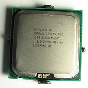
Intel Core 2


The Core 2 brand refers to a range of Intel's consumer 64-bit x86-64 single-, dual-, and quad-core CPUs based on the Intel Core microarchitecture. The single- and dual-core models are single-die, whereas the quad-core models comprise of two dies, each containing two cores, packaged in a multi-chip module.[1] The introduction of Core 2 relegated the Pentium brand to the mid-range market, and reunified laptop and desktop CPU lines, which previously had been divided into the Pentium 4, Pentium D, and Pentium M brands.

The Core microarchitecture returned to lower clock rates and improved the usage of both available clock cycles and power when compared with the preceding NetBurst microarchitectue of the Pentium 4/D-branded CPUs.[2] The Core microarchitecture provides more efficient decoding stages, execution units, caches, and buses, reducing the power consumption of Core 2-branded CPUs, while increasing their processing capacity. Intel's CPUs have varied wildly in power consumption according to clock rate, architecture, and semiconductor process, shown in the CPU power dissipation tables.

The Core 2 brand was introduced on July 27, 2006,[3] comprising the Solo (single-core), Duo (dual-core), Quad (quad-core), and in 2007, the Extreme (dual- or quad-core CPUs for enthusiasts) version.[4] Intel Core 2 processors with vPro technology (designed for businesses) include the dual-core and quad-core branches.[5]

Mendocino

Wednesday, July 15, 2009


The Mendocino Celeron, launched 24 August 1998, was the first retail CPU to use on-die L2 cache. Whereas Covington had no secondary cache at all, Mendocino included 128 kiB of L2 cache running at full clock rate. The first Mendocino-core Celeron was clocked at a then-modest 300 MHz but offered almost twice the performance of the old cacheless Covington Celeron at the same clock rate. To distinguish it from the older Covington 300 MHz, Intel called the Mendocino core Celeron 300A.[6] Although the other Mendocino Celerons (the 333 MHz part, for example) did not have an A appended, some people call all Mendocino processors Celeron-A regardless of clock rate.

The new Mendocino core Celeron was a good performer from the outset. Indeed, most industry analysts regarded the first Mendocino-based Celerons as too successful—performance was sufficiently high to not only compete strongly with rival parts, but also to attract buyers away from Intel's high-profit flagship, the Pentium II. Overclockers soon discovered that, given a high-end motherboard, the Celeron 300A could run reliably at 450 MHz. This was achieved by simply increasing the Front Side Bus (FSB) clock rate from the stock 66 MHz to the 100 MHz clock of the Pentium II. At this frequency, the Mendocino Celeron rivaled the fastest x86 processors available.[6]
At the time on-die cache was difficult to manufacture; especially L2 as more of it is needed to attain an adequate level of performance. A benefit of on-die cache is that it operates at the same clock rate as the CPU. All other Intel CPUs at that time used motherboard mounted or slot mounted secondary L2 cache, which was very easy to manufacture, cheap, and simple to enlarge to any desired size (typical cache sizes were 512 kiB or 1 MiB), but they carried the performance penalty of slower cache performance, typically running the FSB at a frequency of 60 to 100 MHz for motherboard mounted L2 cache. The implementation of the Pentium II's 512 kiB of L2 cache was unique at the time, comprising moderately high-performance L2 cache chips mounted on a special-purpose board alongside the processor itself, running at half the processor's performance and communicating with the CPU through a special backside bus. This method of cache placement was expensive and imposed practical cache-size limits, but allowed the Pentium II to be clocked higher and avoided front side bus RAM/L2 cache contention typical with motherboard-placed L2 cache configurations.[7]

Over time, newer Mendocino processors were released at 333, 366, 400, 433, 466, 500, and 533 MHz. The Mendocino Celeron CPU came only designed for a 66 MHz frontside bus, but this would not be a serious performance bottleneck until clock rates reached higher levels.

The Mendocino Celerons also introduced new packaging. When the Mendocinos debuted they came in both a Slot 1 SEPP and Socket 370 PPGA package. The Slot 1 form had been designed to accommodate the off-chip cache of the Pentium II and had mounting problems with motherboards. Because all Celerons are a single-chip design, however, there was no reason to retain the slot packaging for L2 cache storage, and Intel discontinued the Slot 1 variant: beginning with the 466 MHz part, only the PPGA Socket 370 form was offered. (Third-party manufacturers made motherboard slot-to-socket adapters (nicknamed Slotkets) available for a few dollars, which allowed, for example, a Celeron 500 to be fitted to a Slot 1 motherboard.) One interesting note about the PPGA Socket 370 Mendocinos is they supported symmetric multiprocessing (SMP), and there was at least one motherboard released (the ABIT BP6) which took advantage of this fact.

The Mendocino also came in a mobile variant, with clock rates from 266, 300, 333, 366, 400, 433, 466, 500, 533, and 600 MHz.

In Intel's "Family/Model/Stepping" scheme, Mendocino CPUs are family 6, model 6 and their Intel product code is 80524. These identifiers are shared with the related Dixon Mobile Pentium II variant.

Covington


The first Covington Celeron was essentially a 266 MHz Pentium II manufactured without any secondary cache at all.[4] Covington also shared the 80523 product code of Deschutes. Although clocked at 266 or 300 MHz (frequencies 33 or 66 MHz higher than the desktop version of the Pentium w/MMX), the cacheless Celerons were a good deal slower than the parts they were designed to replace.[3] Substantial numbers were sold on first release, largely on the strength of the Intel name, but the Celeron quickly achieved a poor reputation both in the trade press and among computer professionals.[5] The initial market interest faded rapidly in the face of its poor performance and with sales at a very low level, Intel felt obliged to develop a substantially faster replacement as soon as possible. Nevertheless the first Celerons were quite popular among some overclockers, for their flexible overclockability and reasonable price.[3] Covington was only manufactured in slot 1 SEPP format.

Celeron


The Celeron brand is a range of x86 CPUs from Intel targeted at budget personal computers, with the motto, "delivering great quality at an exceptional value".

Celeron processors can run all IA-32 computer programs, but their performance is somewhat lower when compared to similar, but higher priced, Intel CPU brands. For example, the Celeron brand will often have less cache memory, or have advanced features purposely disabled. These missing features have had a variable impact on performance. In some cases, the effect was significant and in other cases the differences were relatively minor. Many of the Celeron designs have achieved a very high "bang for the buck", while at other times, the performance difference has been noticeable. For example, some intense application software, such as cutting edge PC games, programs for video compression, video editing, or solid modeling (CAD, engineering analysis, computer graphics and animation, rapid prototyping, medical testing, product visualization, and visualization of scientific research),[1] may not perform as well on the Celeron family. This has been the primary justification for the higher cost of other Intel CPU brands versus the Celeron.

Introduced in April 1998,[2] the first Celeron branded CPU was based on the Pentium II branded core. Subsequent Celeron branded CPUs were based on the Pentium III, Pentium 4, Pentium M, and Core 2 Duo branded processors. The latest Celeron design (as of January 2008[update]) is based on the Core 2 Duo (Allendale). This design features independent processing cores (CPUs), but with only 25% as much cache memory as the comparable Core 2 Duo offering.